Request A Quote
- Availability:
- 1-3+ Weeks - ETA

Purchase Protection
Every Order is Protected By BuySafe
Our commitment to sustainability ensures that every purchase supports responsible operations and a healthier planet.
SSL Secure Payment
We make sure your orders are processed as quickly as possible - stocked products are shipped next business day - Vendor direct ship products are processed directly with vendors with vendor leadtime.
Express Shipping
Price Match Guarantee

Your payment is secure
Your privacy and security are our top priority. Our advanced encrypted payment system protects your information during every transaction.

Get expert help
Our team of experienced professionals is always ready to help.
Product Details
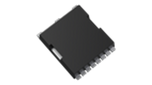
Toshiba 650V 3rd Generation SiC MOSFETs In Surface-Mount TOLL Package -TW083U65C
Experience unparalleled efficiency and performance in your power electronics designs with the Toshiba TW083U65C, a cutting-edge 650V Silicon Carbide (SiC) MOSFET. This 3rd generation device leverages Toshiba's advanced technology to deliver superior switching characteristics and reduced losses, making it ideal for a wide range of demanding applications.
Housed in a surface-mount TOLL (TO-Leadless) package, the TW083U65C offers excellent thermal performance and minimizes board space, enabling compact and efficient designs. Its robust construction ensures reliability and longevity, even under harsh operating conditions.
The new products are Toshiba’s 3rd generation SiC MOSFETs in a general-purpose surface-mount TOLL package, which reduces device volume by more than 80% compared to through-hole packages such as TO-247 and TO-247-4L(X), and improves equipment power density.
The TOLL package also offers lower parasitic impedance than through-hole packages, which helps to reduce switching losses. As a 4-terminal package, a Kelvin connection can be used as the signal source terminal for the gate drive. This reduces the influence of inductance in the source wire within the package, achieving high-speed switching performance;
The TW048U65C is housed in a surface-mount TOLL (TO-Leadless) package, providing excellent thermal performance and enabling compact designs. It's ideally suited for applications such as:
- Switched-mode power supplies in servers, data centers, communications equipment, etc.
- EV charging stations
- Photovoltaic inverters
- Uninterruptible power supplies
Key Features
(1) Chip design of 3rd generation (Built-in SiC schottky barrier diode)
(2) Low diode forward voltage: VDSF = -1.35 V (typ.)
(3) High voltage: VDSS = 650 V
(4) Low drain-source on-resistance: RDS(ON) = 83 m
Ω (typ.)
(5) Less susceptible to malfunction due to high threshold voltage: Vth = 3.0 to 5.0 V (VDS = 10 V, I
D = 0.6 mA)
(6) Recommended gate - source drive voltage: VGS_on = 18 V, VGS_off = 0 V
(7) Enhancement mode
Absolute Maximum Ratings
| Characteristics | Symbol | Rating | Unit |
|---|---|---|---|
| Drain-Source voltage | VDSS | 650 | V |
| Gate-Source voltage | VGSS | +25/-10 | V |
| Drain current | ID | 28 | A |
| Power Dissipation | PD | 111 | W |
Electrical Characteristics
| Characteristics | Symbol | Condition | Value | Unit |
|---|---|---|---|---|
| Gate threshold voltage (Max) | Vth | - | 5.0 | V |
| Gate threshold voltage (Min) | Vth | - | 3.0 | V |
| Drain-Source on-resistance (Typ.) | RDS(ON) | |VGS|=18V | 83 | mΩ |
| Input capacitance (Typ.) | Ciss | - | 873 | pF |
| Total gate charge (Typ.) | Qg | - | 28 | nC |
 DATA SHEET
Shipping & Return
Return Policy
You need to have a Return Authorization (RA) number before returning any products to HSSL Technologies.
For a hard copy of this form and a shipping label, please include your request in the form below.
You can also request an RA online by submitting an RA Request via email. Once you have provided HSSL Technologies with the appropriate information, we will contact you with an assigned RA number.
Defective or DOA Products
DOA or defective products are returned for REPLACEMENT ONLY with the same product/model. Deviations from this policy may result in a 20% Returns Processing Service Charge.
- Defective products must be in the original factory carton with all original packing materials.
- The Return Authorization number must be on the shipping label, not the carton. Please do not write on the carton.
- Returns must be shipped freight prepaid. Products received freight collect, without an RA number, or not approved for return will be refused.
- Return Authorization numbers are valid for fourteen (14) days only. Products returned after expiration will be refused.
- HSSL credits are based on the purchase price or current price, whichever is lower.
General Return Terms
You may return most new, unopened items within 30 days of delivery for a full refund. We will also pay return shipping costs if the return is a result of our error (e.g., you received an incorrect or defective item).
You should expect to receive your refund within approximately six weeks of giving your package to the return shipper. This period includes:
- 5–10 business days for us to receive your return from the shipper
- 3–5 business days for us to process your return
- 5–10 business days for your bank to process the refund
If you need to return an item, please Contact Us with your order number and product details. We will respond quickly with instructions for returning items from your order.
Shipping Policy
We can ship to virtually any address in the world. Note that there are restrictions on some products, and certain products cannot be shipped to international destinations.
When you place an order, we will estimate shipping and delivery dates based on the availability of your items and the shipping options you select. Depending on the provider, estimated shipping dates may appear on the shipping quotes page.
Please also note that shipping rates for many items are weight-based. The weight of each item can be found on its product detail page. To reflect the policies of the shipping companies we use, all weights will be rounded up to the next full pound.
Has my order shipped?
Click the "My Account" link at the top right hand side of our site to check your orders status.
How do I change quantities or cancel an item in my order?
Click the "My Account" link at the top right hand side of our site to view orders you have placed. Then click the "Change quantities / cancel orders" link to find and edit your order. Please note that once an order has begun processing or has shipped, the order is no longer editable.
How do I track my order?
Click the "My Account" link at the top right hand side of our site to track your order.
My order never arrived.
Click the "My Account" link at the top right hand side of our site to track your order status. Be sure that all of the items in your order have shipped already. If you order displays your Package Tracking Numbers, check with the shipper to confirm that your packages were delivered. If your packages each show a status of "delivered", please contact customer service for assistance.
An item is missing from my shipment.
Click the "My Account" link at the top right hand side of our site to track your order status. Be sure that all of the items in your order have shipped already. If you order displays your Package Tracking Numbers, check with the shipper to confirm that your packages were delivered. If your packages each show a status of "delivered", please contact customer service for assistance.
My product is missing parts.
Click the "My Account" link at the top right hand side of our site to track your order status. Be sure that all of the items in your order have shipped already. If you order displays your Package Tracking Numbers, check with the shipper to confirm that your packages were delivered. If your packages each show a status of "delivered", please contact customer service for assistance.
When will my backorder arrive?
Backordered items are those which our suppliers are unable to predict when they will have more in stock, but as soon as they do, we will be able to ship the item to you.
Warranty
Why Choose HSSL?
We connect businesses with the right technology solutions to power growth, security, and efficiency.

Expertise
Backed by years of industry knowledge, our specialists understand the challenges modern businesses face.

Partnerships
We collaborate with top-tier technology providers to bring you innovative & high-performance products.

End-to-End Support
Our dedicated support ensures your systems stay optimized, secure, and ready for what’s next.

Scalable Solutions
Our adaptive approach ensures your IT infrastructure evolves seamlessly as your business expands.
Expert in IT & Security Solutions
At HSSL, we specialize in delivering cutting-edge IT infrastructure, cloud, and cybersecurity services that empower businesses to thrive in a digital-first world. Our trusted professionals provide reliable insights on:
-
Digital Transformation Strategy
Empowering businesses to adapt and grow through modern, secure, and scalable digital infrastructure.
-
Advanced Cybersecurity
Protecting your organization from digital threats with proactive monitoring and smart security frameworks.
-
Cloud & Infrastructure Management
Optimizing cloud performance and IT operations for seamless scalability and improved business agility.
-
Data Backup & Recovery
Ensuring business continuity through secure data management, automated backups, and rapid recovery solutions.
-
Network & Endpoint Solutions
Delivering secure, high-performance networking systems that keep your business connected and efficient.
-
Technology Consulting
Guiding organizations toward smarter IT investments and solutions that align with their long-term goals.
You May Also Like


Jabra Evolve3 75 MS, Link390c, Black, WLC chrg - 37599-999-889

Jabra Evolve3 75 UC, Link390a, Black, WLC Chrg - 37599-989-989